Designmaster from Groupdiy sent me an interesting PM regarding my Power Distribution plans.
"How do you want to make the 5V for the ADC. For example the PCM4202 needs 65mA for the 5V analog voltage. You have 18V going to the board.
This will result in over 0.8W of dissipation loss and will generate heat which is not the best for thermal noise performance. I would recommend an additional supply rail with lets say more than 5V for the ADC or DAC may be 7V than you have the option to use a 5V voltage regulator on the board and than you will get a nice and low-noise supply.
How about 48V for phantom powering if you plan to go for a MIC Input board with integrated ADC? "
That made me think a little further. My initial plan was to only have a single "Hard Drive" type power connector. However, I soon needed more connectors (5.. not 4... )
So, a little more thought, means that I could have a 4 way digital connector and a separate analog connector. It would also means that my supply boards can be completely separate on the board.
Nice :)
Tuesday, November 21, 2006
Tuesday, November 14, 2006
Getting back to basics
I've been so distracted by new projects recently, that I forget why I did all this:
I wanted an AD-DA with ADAT connectivity. Simple. Easy.
A recent post on Groupdiy by Svart reminded me of this. I've spent so much time trying to get the interconnect sorted, that I lost sight of what I wanted.
So -- with the interconnect almost sorted - it'll soon be time to get back to what I really wanted to do :)
3 actions:
1 - complete standardised interfconnect
2 - Get PCM4204 and PCM4104 EVM's and ADAT Cards made - test.
3 - If successful, optimise EVM's for easy DIY production. :)
Tuesday, October 24, 2006
Motherboard connectors (attempt 1)
To make the system work with ribbon connectors etc, here's a suggested pin requirement. Please comment...
it makes 19x2 in total... 19x 0.1" = 1.9" long, 0.2" wide connector.
POWER
+18VDC - Analog
AGND
-18VDC - Analog
AGND -
Analog12VDC - Digital Supply
DGND
Requirement: 3x2 0.1" connector
Clocks
FS - Typically 44.1kHz
DGND
256fS - 256xSampling Frequency
DGND
512fS - 512xSampling Frequency
DGND
Requirement: 3x2 0.1" Connector
Control
SPI - CS (SPI Chip Select)
DGND
SPI - SCLK (SPI Serial Clock)
DGND
SPI - DIN (SPI Data In)
SPI - DOUT (SPI Data Out)
SCK - I2C (I2C Clock)
DGND
SDA - I2C (I2C Data)
DGND
Requirement: 5x2 0.1" Connector
Audio (Left Justified)
LRCK (Typically the word clock brought in from the clock source)
DGND
BCK (128fS or 256fs)
DGND
Data (Left Justified Data)
DGND
AES+ (S/PDIF or AES Data)
DGND
AES- (S/DPIF or AES Data)
DGND
EXTRA1
DGND
EXTRA2
DGND
EXTRA3
DGND
Requirement: 8x2 0.1" Connector
API 500 series
I recently did some work in Eagle (Cad software for PCB's) to create a library for the API500 (http://www.apiaudio.com/5006b.html) standard.
http://www.prodigy-pro.com/forum/viewtopic.php?t=18715
This standard looks to be an awsome standard for DIY'ers to standardise around, although I do have some concern for it's ability to deal with digital audio.
For instance, the only supplies in the standard are ±16VDC supplies. This is obviously aimed at the analog signal chain supplies. Not knowing enough about noise in digital and analog systems makes me concerned that a digital product could really spoil the supply, not only in the card that contains the analog and digital, but also the rest of the box (the other 5 units in the lunchbox).
Such "analysis" of the card and it's format really made be re-evaluate the motherboard plan that I was doing, but also look for an alternative sub-rack system. A post on group-diy pointed to something called a Frac Rak - made by Paia Electronics. http://www.paia.com/fracrak.htm
Someone mentioned in the thread that the Paia board wasn't strong enough in comparison to the API lunchbox. However, a little more research into the Fracrak shows that it is incredibly popular in the DIY Synth market. Those folks are pretty much doing what we're doing here, except that their boxes are more fixed in place (at the geeks home) :-)
I kept on chewing onthis thought, wondering on how I could strengthen the box, how I could make it so that card edge connectors could remain in place, even when the unit is under stress.
The conclusion I came to was that if you were really serious about making the unit mobile, you'd flight case it on its own (in an SKB like case). AS for card edge connectors... forget it. I'm still tempted to use ribbon connectors with 0.1" spacings. That way, if these is some bending, the card mounted vertically (e.g. the mic amp) isn't going to put pressure on horizontal board (the motherboard).
In the case of the system that will mainly be individual cards that can have audio chained from one to the other, then there isn't so much of a need for a control processor or CPLD. The main use for a motherboard system of such a kind is in the distribution of shared resources - power, clocks, control (SPI and I2C) etc.
My design experience in these fields is limited, however, I have seen many implementations in Pro Systems, and asked many a question. Any comments you have are appreciated.
Cheers,
R
Friday, August 25, 2006
Motherboard Topology
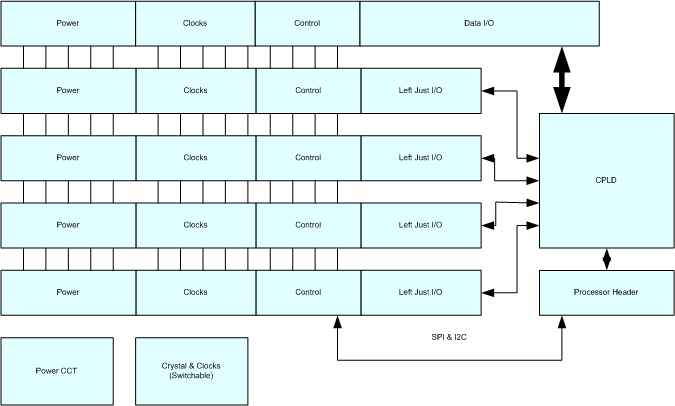
So - block diagram time.... the system can be built on a "motherboard" type architecture.
Such an architecture keeps 2 thngs in mind:
- The cards can work remotely - without the motherboard.
- Any mix of cards can be incorporated
- The CPLD can work as a "router" or a crosspoint switch.
Friday, August 18, 2006
Ahhh... after quite a delay, the boy is back in town :)
For those that have followed this project, the delay has been blamed on my recent move to Texas with work. Let's just say that the difference between the UK and Texas is bigger than I expected :)
The new job is very relevant to the parts that are being dicussed in the projects on this page and on GroupDiy... in fact, I do wonder how many of my customers actually read groupdiy :)
Anyway - I digress...
I've had to relearn my own Schematic. (I always hate that...). I figured it's worth making a point of the pinouts for the connectors in the circuit.
ADC Connectors:
Pin Function Direction
1 Data In
2 DGND
3 256fS Out
4 DGND
5 64fS Out
6 DGND
7 Word ClockOUT
8 DGND
9 DGND
10 DGND
DAC Connectors:
Pin Function Direction
1 Data OUT
2 DGND
3 256fS Out
4 DGND
5 64fS Out
6 DGND
7 Word ClockOUT
8 DGND
9 DGND
10 DGND
As the initial intention - This is a modular design based around a modular system. More on the Modular system in posts to come.
Cheers
R
Friday, November 25, 2005
Schematic update
Schematic finally updated...
Changelog:
-10uF Tant Caps added for decoupling
-Driver Buffers Changed to sn74ahc541
-SIL Resistors changed to DIL for ease of layout.
-Onboard crystals added, with jumpers for switching - can also be connected to switches for a frontpanel.
http://www.tendolla.com/diyinterface/ADATWC%20-%2025nov05v2.pdf
CPLD Research
Following some info from a few people on groupdiy (Designmasta and tmbg) I've had a look at the Xilinx range of CPLD's - and I must agree, for more advanced boards (i.e. a next generation board of this type?) then a cpld is a definite possibility.
I think the main use of a CPLD in a board of this type is more a routing matrix for now though, or possibly a routing matrix with some extra functions.
Programming them looks relatively simple (you need a parallel port on you're PC from the looks of things, and the right cable that comes with the $50 starter kit).
Anyway, I'm hoping to sit down tonight and do the schematic updates discussed.
cheers.
R
Wednesday, November 23, 2005
Decisions based on feedback
Based on the feedback so far from MCS and Designmaster - these changes are to be made to the Schematic
Changes to make
Changes to make
- Add 10uF Tant Capacitors to "high current" driver devices.
- Convert the 4way output pins to 10way ribbon connectors using a DGND connection for every other pin. That will also allow me to send another clock derivative.
- Add a "clock source select" section - allowing the user to select a 44.1KHz crystal circuit or 48KHz circuit.
Investigation to make
CPLD use for changing settings - how easy can it be? Is it within the grasp of the DIY'er?
Feedback on initial schematic
Good feedback today from both MCS and Designmaster on the initial schematic posted on www.groupdiy.com
From Designmaster:
I would add a 10uF Tantalum capacitor for each device in parallel to the 100nF 8 buffers are a lot. typical 40pF load. You can also use ICS551 which is a 1 to 4 buffer, I know keep it easy. But it should work, you may have to play a little with the value of the serial resistor and the kind you distribute the signals on the PCB. Why don't you go for a FPGA or on the Wordclock board for a CPLD (XC9572XL)? Would make your life much easier and you can get ride of a lot of jumpers.
I only saw 100nF caps but by driving "heavy" loads where does the energy came from. First from the 100nF right but than?? You only have a 2 layer board and you will need at least 2 or better 3 of 10uF Tantalum. One right at the connector and the others around on the board.
From MCS:
Wordclock should be an Ethernet-like bus with T-connectors and a terminator at the end - but I don't know. You would need a terminator when the input is not used, but I guess most people have some Ethernet terminators available...
I'm not sure the four outputs need buffers - my board works fine without at least. But the bitclock, wordclock and masterclock do of course.
I normally like to put ground pins between the signals on the headers to keep them from interfering (a la SCSI). I actually use 10-pin connectors with a lot of ground pins. But that's mostly because cables with 10-pin IDC connectors are so easy to make.
Here's my tested OptoGen schematic BTW: http://stiftsbogtrykkeriet.dk/~mcs/OptoGen_sch.gif
Tuesday, November 22, 2005
Finally,
here's the first schematic - it still needs a lot of work though - any comments (corrections please!)
http://www.tendolla.com/diyinterface/ADATWC%20-%2022nov05.pdf
Cheers
R
here's the first schematic - it still needs a lot of work though - any comments (corrections please!)
http://www.tendolla.com/diyinterface/ADATWC%20-%2022nov05.pdf
Cheers
R
PCM4202 EVM Study
PCM4202 EVM users guide
I've been looking at this EVM to see how things are done on TI's EVM's - looking for good design guides.
100R Resistors on outputs:
It looks like there are 100 ohm resistors (in series, NOT tied to ground) on every logic device's output. This (according to MCS on Groupdiy) is for termination reasons and other factors.
SN74ALVC245PW
Is used as a buffer/line driver for the 3.3V devices on the board.
For 5V devices
SN74ACT244
SN74ABT244A
look to be good replacements, but they need to support up to 256fS (around 25MHz).
The CDC337 looks very interesting - it's a Clock driver that can support a single clock in, the 4 out, plus another 4 at half the rate. So if we take 256fS as one clock rate, we can get 128fS out as well.
More as I think of it. :)
Cheers
R
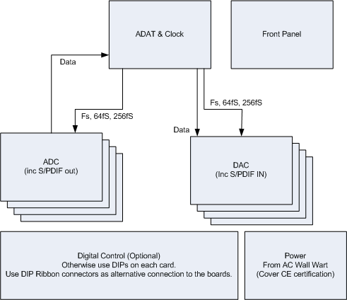
ADAT Card and ADC
Ahhhh... let me see, where do I begin... This project is happening over at http://www.groupdiy.com. The actual thread is: http://www.prodigy-pro.com/forum/viewtopic.php?p=135492#135492
The Idea so far is:
Stereo ADC Card118dB 24bit, working either from onboard crystals to generate clocks to drive an S/PDIF Transmitter up to 96KHz or in a slave mode that will support up to 48KHz.Basically, it can act a standalone ADC with S/PDIF or as part of an ADAT 8 channel ADC.
ADAT Card
Can generate all clocks from an external word clock or ADAT input. 4 connectors onboard to distribute clocks (Fs, 128fS and 256fS to the adc card) and bring back the Data from each of the stereo ADC's. The card will then convert the data from each stereo ADC into a single ADAT stream.
On the ADAT card there are 8 external 4 way connectors...
4x [data out, Wordclock, 256xWordclock and 64x Wordclock]
4x [data in, Wordclock, 256x Wordclock and 64x Wordclock]
Each of these are buffered for 5V use to go over 0.1" connectors to ADC cards or DAC cards.
The I/O on the ADAT card will be +5V - this should help with noise performance as well.
Thursday, May 19, 2005
Guitar FX.
today has been a day of 2 sides...
I'm getting more excited about getting these fx pedals done. I've currently finished 3 pcb's that I can get done together on one big one out in Bulgaria with Olimex. http://www.olimex.com
The 3 pedals that are done are: PNP Fuzz Face, Big Muff and the Seamoon Funk Machine. Each is well under 5cm x 5cm (see below) -- each of the fx are going on dual sided PCB to make them as small as possible.
Fuzz Face is: 35mm x 20mm
Big Muff is: 50mm x 40mm
Funk Machine: 30mm x 40mm
Subscribe to:
Posts (Atom)

