Friday, August 25, 2006
Motherboard Topology
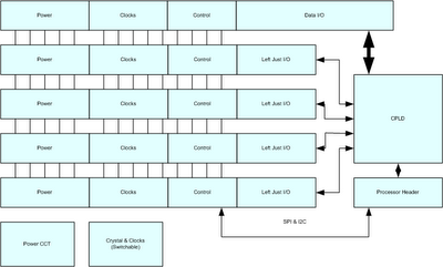
So - block diagram time.... the system can be built on a "motherboard" type architecture.
Such an architecture keeps 2 thngs in mind:
- The cards can work remotely - without the motherboard.
- Any mix of cards can be incorporated
- The CPLD can work as a "router" or a crosspoint switch.
Friday, August 18, 2006
Ahhh... after quite a delay, the boy is back in town :)
For those that have followed this project, the delay has been blamed on my recent move to Texas with work. Let's just say that the difference between the UK and Texas is bigger than I expected :)
The new job is very relevant to the parts that are being dicussed in the projects on this page and on GroupDiy... in fact, I do wonder how many of my customers actually read groupdiy :)
Anyway - I digress...
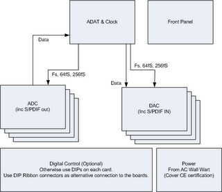
I've had to relearn my own Schematic. (I always hate that...). I figured it's worth making a point of the pinouts for the connectors in the circuit.
ADC Connectors:
Pin Function Direction
1 Data In
2 DGND
3 256fS Out
4 DGND
5 64fS Out
6 DGND
7 Word ClockOUT
8 DGND
9 DGND
10 DGND
DAC Connectors:
Pin Function Direction
1 Data OUT
2 DGND
3 256fS Out
4 DGND
5 64fS Out
6 DGND
7 Word ClockOUT
8 DGND
9 DGND
10 DGND
As the initial intention - This is a modular design based around a modular system. More on the Modular system in posts to come.
Cheers
R
Subscribe to:
Posts (Atom)